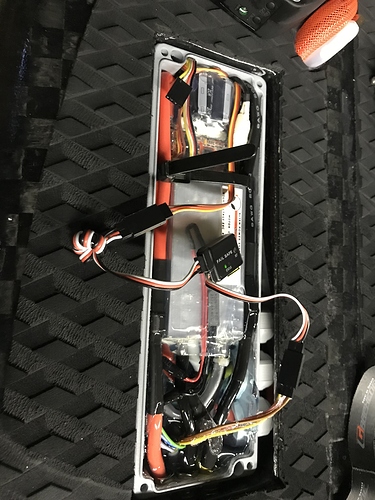
Build all in one

yeah in theory, you just need a MCU, some gatedriver, amplifier and some FETs. But I think it is a quite long way till you have something reliably working…

That’s exactly what the VESCs do, but with other DRV chips.

So I guess you are using 4.xx design?!
The D-Pack package used on both sides is really bad for heat transfer (since most of the heat is brought to the back side, so onto the PCB and against the otherside FET). All newer versions use Direct FET package and only one side with FETs, so maybe upgrading to Focbox, Vesx, Escape, Bbox or V6 is worth it.

or use something isolating fluid…

only the old versions…all newer use Direct FETs…

I used a VESC-X before. I tried it with water cooled heatsink and also a large heatpipe CPU cooler mounted to the housing.In the end i tried small aluminium heat sinks glued to the individual Fets. The latter one had the best air cooling, measured by performance with D-current and slowly turning motor/prop in water. After some hours driving it destroyed one direct FET and thereby also small connections on the PCB. I had set the temperature by 10°C higher than recommended, so maybe its my fault.
I could not get more power through it than with the VESC 4.12 with heatpipes now. 2.4kW was the maximum, quickly dropping to 1.7 …1.3kW.
So the question remains if the direct FET approach using thermal pads is really a good way? The area to transfer the heat is really small with those direct FETs. Most of the heat will go into the PCB and indirectly through the thermal pad into the housing.
And there is another problem: The PCB traces and the shunts and also the capacitors heat up as well and need some cooling at least by forced air flow.

Yesterday one of the capacitors of the VESC 4.12 just popped after charging without any current flow. I wonder what that means? Is my ripple current too high? I will cut out the BMS for the driving current and install larger capacitors. Maybe i get better results then.

how did you attach them mechanically? I guess pressure is quite important if you use anything like thermal paste/pads.

well, years ago we made some fun by using some “high” voltage to let some caps plopp. But I guess if you were over the cap rating you would have had other problems at the main PCB.

But if you are replacing your caps anyway you might have a look here. Also he has a nice heat sink design for the vesc 4.xx (he uses 4.7, but that doesnt matter).

What cap did fail? I have 2 assembled Vescs (4.12 modiified) and use 5 low ESR 470uF input caps, I have not killed any of cap yet. I connect my batteries with a 2 Ohm precharge resitor now, as I killed a vesc once with too long PSU wires and no precharge resistor.
So you would advise against directFET Vescs?
A picture of the failure and/or your cooling soultion would be great.

No, i do not want to advise against direct fets. I only think it makes things more complex. There are several cooling concepts for transistors, some are going through the PCB and some do not. If you place all Fets on same side of PCB, you can have masses of Vias to the back side and you could cool them easily because you have a very even surface (if you do not populate it). This makes it easy to attach heat sink with a very thin gap, still electric isolating. The problem with miniaturisation is the missing area and cross section leading to higher current and thermal flow density. We need something more rugged, the current flow density through VESC PCB is very high, especially with version X. More copper for those long lasting current!

The caps were getting hot. That might be the failure. Overload by too high resistance and inductance of source might have led to an overload situation. The middle one of the 3 680µF popped, at cool situation with around 50V without any current flow, it was around an hour sitting in this situation while balancing. The charging power supply is nice and was off at that time.

For insiders: The problem about testing with D-current using VESC with motors slowly turning while having masses of ohmic copper losses is, that the Capacitors and the DC-link circuit are not tested. Also the switching voltage losses inside the Fets is not considered correctly. I estimate the real life losses of my VESC 100% more than in D-current test run. Additionally to the losses inside the cells, cables, fuses, BMS, relays.

1 Like

What do you think about totally epoxying the ESC and keep it underwater? Might it work in terms of efficient cooling? I have doubts about electrical isolation capability of the epoxy on one side and resisting to thermal power dissipation on another side.

I have attempted something along those lines in the thread Direct drive outrunner with direct water cooling - #44 by Flo - Propulsion System (Motor, Gears) - FOIL.zone. I used a standard isolation pad (glasfibre silicone foil) to get rid of any conducting path between the pipe and the transistors.
So far this was working quite welll in air, but I hesitate to seal it up for underwater use. Making it servicable is hard. That’s why I went back to a more conventional watercooling system using pumps.

I used a two component gel, it is used as electrical insolation and it helps transmit heat to the aluminum case. And on the plus side you can remove it if needed, just keep the usb accessible in case you want to flash the esc.

2 Likes

Hi @Clarin, what is the name of that two component gel? Can you share it please?

I got it in Hornbach, it came with a plastic box and the quantity of gel is just enough. It’s like slime gel, just more sticky, hopefully I won’t need to get my esc out :wink:
https://www.hornbach.ch/shop/Manchon-de-cable-en-gel-pour-cable-plastique-6-16-mm2/8448311/article.html

Here is a similar one: https://www.fastlec.co.uk/mp-gel100-wiska-mp-gel-100-1-litre-multipurpose-for-electrical-insulation.html

1 Like

I studied the bbox, focbox, escape, 4.12 and they all use the same schematic in general, two shunts, DRV8302. The main difference are the FETs and the mounting and connection of the caps. There are some newer designs like Vesc 6 (trampa) using direct fets with nice housing but bad thick thermal cushions between the Fets and cool housing. I have not analysed it because its overpriced for my budget. The problem seems to be always the same:
You have an amount of electrical potentials, typically 5, which are the motor terminals and the supply voltage, ground, which must be isolated under all circumstances.
So there has to be some insulation between the cool housing and the Fets, also allowing to even out mechanical tolerances.
VESC4.12 fet https://www.infineon.com/dgdl/irfs7530-7ppbf.pdf?fileId=5546d462533600a40153563a9d1e21d8
The direct fets used are https://www.infineon.com/dgdl/irf7749l2pbf.pdf?fileId=5546d462533600a40153560445e71ca2
Later VESC design use even smaller Fets:
https://www.onsemi.com/pub/Collateral/NTMFS5C628NL-D.PDF

The original VESC 4.12 was very compact in its current paths, the high side fets, as always, share their cooling plate, the Drain, which has supply potential. Their Source is directly connected to the motor terminal and because its double sided also the low side fets drain cooling plate. The only disadvantage are the shunts, which need to be mounted on the PCB, with 1mOhm, they are a pain regarding thermal load to the PCB. The heat cannot be transferred from there. So i added some cooling where it is possible to mount without changing the layout or dissoldering the fets.


The problem is, that the PCB transferring the heat is very thin, typically 70µm, which generates heat itself. Even 105µm at 100A is too small to transfer heat in a valuable amount. At least the PCB is now cooled and sucks the heat from the Drain cooling of the fets.
The newer VESC designs all use direct fets with the promise to enhance the cooling dramatically.
Now, lets compare some aspects of the data sheets.
irfs7530 : Max R_DS_ON: 1.4mOhm at 100A ; R_JC: 0.4K/W, MaxP_D: 375W
irf7749: Max R_DS_ON: 1.5mOhm at 120A (2%Dutycycle); R_JCan: 1.2 K/W MaxP_D: 125W
NTMFS5C628: Max R_DS_ON: 2.4mOhm at 50A; R_JC: 1.3K/W; MaxP_D: 110W, two are used in parallel, so you get doubled or halved values.
The effective R_DS_ON is almost the same, although the oldest parts wins. Thermal resistance is definitely worser for the newer parts, and the elder irfs7530 can be used as a heater, it has the largest footprint.

So the newer designs have not made so much out of the benefit of direct top cooling or distributing heat over a larger area. They use a larger PCB area to accomplish the same or even worse performance.

Why is it so?
The ESK8 scene calls for very light material. They have a typical usecase: Accelerate, hold speed with low torque, decelarate. With 3kW you could accelerate to 50km/h within seconds. All the tests of the ESK8 scene are not valuable for us. The peak power demand of a skateboard is similar to the average power demand of a windsurfboard without foil. And honestly: What helps? Power!

What can be done with 4.12 derived designs?
Stabilize the voltage by more capacitors and better wiring, so there is less heat created by the leads, contacts, caps, which surround the esc. The less heat they produce, the more they can take from the PCB.
Get the heat away by air and rib cooler and spread it.
Cancel out the root cause.
What is producing the heat? The R_DS_ON for sure, the shunts, the PCB and the switching losses inside the fets, the latter one can only be changed by the gate driver concept.

Suggestions: Use 0.5mOhm shunts because it seems easy. Use fets with lower R_DS_On. I found one and bought some.

I think i will integrate it to the VESC4.12 by a copper adaptor which acts as a primary heatsink, 1-2mm thick, and as a terminal for all 5 power connections. These copper plates exceed the original PCB around 10-30mm. They can be used to mount cushions, ribbed coolers, heatpipes, watercooler, whatever, with or without insulation. By this the cooling area is multiplied and those supadupa fets can play their role out and deliver 100A continously.
Even an immersed fluid cooling would be possible.
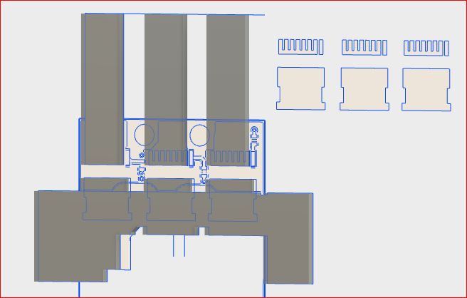
vesc%20example
What do you think?

3 Likes

sounds like a beefed up, cooled cable. But how will you isolate that?
Okay, you spread up the heat produced by the underside of the Fet directly to the “cable”/terminal, but then how will you go on?
I mean, if you put heatpipes or ribbed coolers on top, you will have the same problem with 5 different potentials and isolating all.
Maybe immersed fluid cooling with synthetic (isolating) oil…

2 Likes

This way the middle one of the high side fets will always be hotter than the outer ones, maybe that‘s not a problem but I would calculate that.

1 Like

I finished an example design to make some simulations in fusion for tuned VESC4.12.
I want 100A, i use 0.5mOhm shunts and IPT007 (James, where are you?). I used 2mm Copper plate and i simplified the Mosfets mechanically to their footprints.
For each drain i used 10W, each source 3W, each shunt 5W, overall 88W. Ambient temperature was chosen 50°C to simulate heated situation in a closed air loop cooling inside the closed case with forced air cooling by a fan. I chose a convection of 100W/m^2K (if you have realistic values from your experience, please let me know) and radiation with an albedo of 1 and ambient temperature of 50°C.
The result is amazing to me:


Why amazing?

  1. The shunts are doing the biggest trouble! They heat into the source of the low side fets! Ok, the ground cable is missing in my simulation, but anyhow, they produce a high temperature which is hard to cool at this place.
  2. Uniformity of temperatures inside the 2mm thick copper.
    To analyze it i use the thermal current view:

    The high side fets drain are around 12K hotter than the low side, the middle one of the high side being 1-2K hotter than outer ones. I could add some more area for the high side drain cooler, but i doubt that i can solder it than.
    So the copper is too thick in economical means. But it will serve as an excellent dynamic heat sink.
    I have some experience in soldering very heavy motor cables and also some PCB soldering experience, but soldering 6€ fets to massive copper bars? Never did it before.
    Before i go on to produce these copper parts on my cnc, please give me your best advice.
3 Likes

I think your 13W total losses per FET at 100A motor current is reasonable.̶ ̶̶i̶̶f̶̶ ̶̶y̶̶o̶̶u̶̶ ̶̶c̶̶a̶̶n̶̶ ̶̶k̶̶e̶̶e̶̶p̶̶ ̶̶t̶̶h̶̶e̶̶ ̶̶j̶̶u̶̶n̶̶c̶̶t̶̶i̶̶o̶̶n̶̶ ̶̶t̶̶e̶̶m̶̶p̶̶e̶̶r̶̶a̶̶t̶̶u̶̶r̶̶e̶̶ ̶̶l̶̶o̶̶w̶̶ ̶̶e̶̶n̶̶o̶̶u̶̶g̶̶h̶̶,̶̶ ̶̶b̶̶u̶̶t̶̶ ̶̶i̶̶t̶̶ ̶̶l̶̶o̶̶o̶̶k̶̶s̶̶ ̶̶l̶̶i̶̶k̶̶e̶̶ ̶̶y̶̶o̶̶u̶̶ ̶̶c̶̶a̶̶n̶̶ ̶̶m̶̶a̶̶k̶̶e̶̶ ̶̶i̶̶t̶̶ ̶̶i̶̶n̶̶ ̶̶y̶̶o̶̶u̶̶r̶̶ ̶̶s̶̶i̶̶m̶̶u̶̶l̶̶a̶̶t̶̶i̶̶o̶̶n̶̶.̶̶ ̶̶a̶̶t̶̶ ̶̶1̶̶1̶̶0̶°̶c̶̶ ̶̶t̶̶j̶̶ ̶̶i̶̶t̶̶ ̶̶w̶̶o̶̶u̶̶l̶̶d̶̶ ̶̶a̶̶l̶̶r̶̶e̶̶a̶̶d̶̶y̶̶ ̶̶b̶̶e̶̶ ̶~̶1̶̶7̶̶W ̶… Ah with your IPT007 spies that’s already with the RDSon at 160°C, nice. Unfortunatly I don’t have too much experience with convection. They don’t give practical values in Fluiddynamics and Heat transport lectures :frowning: .

I should have listened to you a little bit more, with my 1mOhm Shunts I burn 10W per shunt (like you told me) and those have only forced air cooling with many obstructions to the airflow… I will calculate if the surface area is enough to get the heat to my watercooler. Fortunately the heat leaked through the PCB to the small 10kOhm NTC on my board to prevent my stupidity from damaging my working ESC. I mean I just assumed the shunts would be fine and didn’t even calculate the losses.
I like your thermal simulation in Fusion, I will have to look into that and maybe get some simulation for may watercooler.

As it seems you don’t have any issues conducting the heat away from the drains of the high side fets, I would advise to not mount the copper plates on the source pins for the HS Fets. This will make it much easier to keep good isolation in operation and it will be easier to assemble. Increase the copper area on the sides instead, if you are worried about convecting the heat away to the air.

On assembling big copper parts on a PCB:
How will you connect the gates to the PCB? I imagine a 2mm gap between the gate contact and the PCB. For source and drain there is the copper plate, obviously. When I flipped the FETs on my other Vesc 4.12 to expose the drains for cooling I used thin isolated copper wire (“Kupferlackdraht”) to connect the FET. As this is quite fiddly with the gate contacts I damaged some fets and (repairable) pulled a pad from the PCB. So I would advise to be careful here and turn the soldering iron down to the temperature needed for the current job.
To desolder the old FETs I always used a temperature controlled heat gun with great succes for PCB and FET recovery. (* I did not measure the performance of the mosfets I have removed and resoldered using this method.) A little leaded solder helped for me sometimes (prototype, no ROHS :slight_smile: ).
I use a circular nozzle on the heat gun with a diameter slightly larger than one FET. I try to somehow evenly preheat the PCB with 110°C air around the complete mosfet section. Then I turn the heat up to over 200°C or higher strongly depending on the distance from the fets. I think some practice is necessary in this area. I use my fathers heatgun which is way overpowered with 1,5 kW, but it’s nice to have the necessary heat flow. I pull the FETs using tweezers and cool them afterwards.

For assembling the copper plates on the PCB i would only aid soldering with a soldering iron if you see areas that need it. As you know the copper conducts the heat way to good to assemble one FET at a time. In my setup the copper plates are perpendicular to the PCB and not flat so I got away with at least assembling one PCB side at a time. I’m not sure if you can do this with your design.
Anyway I would advise to use solder paste and assemble everything in a cool state. Then clamp everything without preventing airflow. Surface tension, airflow and gravity are all nasty enemies when trying to assemble multiple floating copper parts, a PCB and the better part of 40€ in mosfets. You probably know most of this better than I do, but I want to mention some things to think about because trying to keep 5 pieces floating in liquid solder in one place only leads to burnt fingers and suboptimal results.
When everything is in the place it needs to be, heat it up evenly with 110°C airflow and than melt the solder paste with a higher temp. You can use your soldering iron and add some normal solder to let it get sucked into the joints. I tried to mimimze the exposure to the heat of this suboptimal reflow profile by cooling everything rapidly after soldering. I just sprayed denatured alcahol on the heatsink and fets, evaporative cooling works great here. I did not use any additional flux, but it might help for you to ease solder coating. I have a diy hot plate, so I would think about clamping the setup on this heat source for soldering. This is only advisable if you find it necessary to solder both sides at once. That way you only have to worry about one side with the heat gun, but the hot plate will not cool down very fast after the solder has reflowed.

Thanks for sharing your design and simulations. I will now think about cooling my shunts, too. Maybe a quick fix would be to insert a copper bar between the two shunts. I mean where both have the same potential, GND. And then get the heat from there to somewhere or my watercooler. I will have to calculate the heat resistance with the shunt areas. Unfortunately just soldering a big copper bar on top of the shunts will not work here. Maybe i will just add a copper plate on each side and transfer the heat through GF-Silicone pads to my watercooler then.

Hi,

…very interesting your thermal simulation. I was thinking about CNCing most of the power paths out of aluminum in a similar way.

soldering 6€ fets to massive copper bars?

As Flo explained, the easy way to solder is to use solder paste and to heat up everything at once (reflow soldering). One or more thermocouple sensors on the copper parts make things easy. Its even easier if the heat source is closed-loop controlled by a thermocouple.

I use a low cost preheating table to reflow (Aoyue 863, 3 thermocouples and closed loop control), with a glass kitchen pan cover to keep heat close. Using lead free soldering paste, I preheat to 180°C, and once stabilized, I program 250 °C and wait for melting the solder, helping eventually colder spots with a soldering Iron as Flo does.

The advantage of not using a big hot air gun is avoiding blowing away the components.

Smaller PCB preheaters starting at about 100 € and may be sufficient in this case.

Hope that helps,
Bernt

1 Like

Thank you very much for your help. I recognized something was wrong in the simulation results, somehow some parts were unintended unified.
Additonally i changed some parameters, so now its 12W for each Drain, 1W for each source, 5w for each shunt, altogether 88W like before.


So i made the HS cooler larger, reduced the HS source coolers.
I introduced some M2.5 brass screws, to be able to premount the coolers without any mosfet, clampening the screws while solder is fluid. Is this a good idea? Does it help to control the parts? For the LS mosfets source and the shunts this is not possible.
Before i produce this, i will make further simulations of the original 4.12 with 0.5mOhms with irfs7530, immersed cooling. The effort of this copper grave discourages me a little bit. I think i need practical help from someone familiar with such equipment.

Here is a thread where someone has already done a 200A version…

https://vesc-project.com/node/339

Interesting link, i had some contact, but the price is rather high from my opinion.
Today i managed to solder in the kitchen oven, the largest part of the cooling:


I connected with BLDC tool and flashed it and it seems to still work.
I mounted a K-type temperature sensor on the heat sinks hole. Put it in the kitchen oven, waited for 220°C, the PPM input cable desoldered, than i opened the door and let it cool.
It took around 7 minutes. Heat from above to heat the sink and air circulation.
Now i will produce the remaining copper parts.
What could i improve, what do you think?

3 Likes